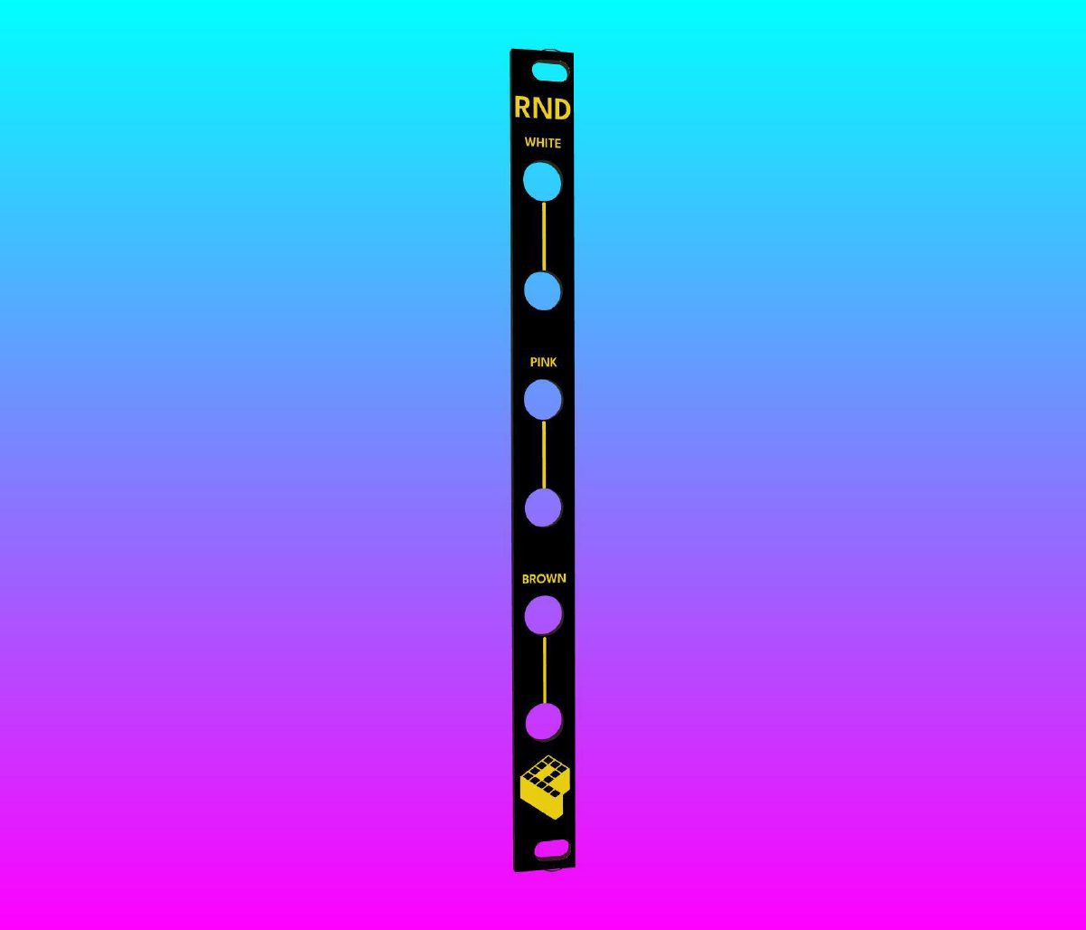
RND is an analog noise source in just 2HP. It generates white noise from a reverse-biased transistor junction and filters it into pink and brown noise. Each of the three outputs has its own level knob. Use it for snares, hi-hats and wind sounds, as a modulation source through a slew limiter or a sample & hold, or as a test signal for filters.
Perfect companion for the VCF, the VCA and the Quantize & Hold module.
Key features#
- Three noise colours: white, pink and brown
- Level knob for every output
- True analog noise from an avalanching transistor junction
- Pink noise with a
-3dB/octslope, brown noise with-6dB/oct - All three outputs at roughly the same loudness
- TL074 quad op-amp,
±12Vpower - Black front panel with ENIG gold-plated lettering and logo
- 2HP wide
Controls#
| Control | Function |
|---|---|
| WHITE | Level of the white noise output |
| PINK | Level of the pink noise output |
| BROWN | Level of the brown noise output |
Each knob sits directly above its output jack. Fully counter-clockwise the output is silent.
Noise colours#
Noise colours describe how the energy of the noise is distributed over the frequency range:
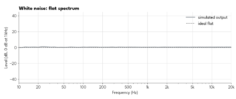
- White noise has the same energy at every frequency. Because each octave contains twice as many frequencies as the one below, white noise sounds bright and hissy. It’s the classic source for hi-hats, snares and “sh” sounds.
- Pink noise loses
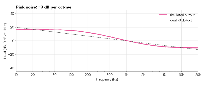
3dBper octave, so every octave carries the same energy. To our ears this sounds balanced, like rain or a waterfall. Pink noise is also used to test speakers and rooms. - Brown noise (named after Brownian motion, not the colour) loses
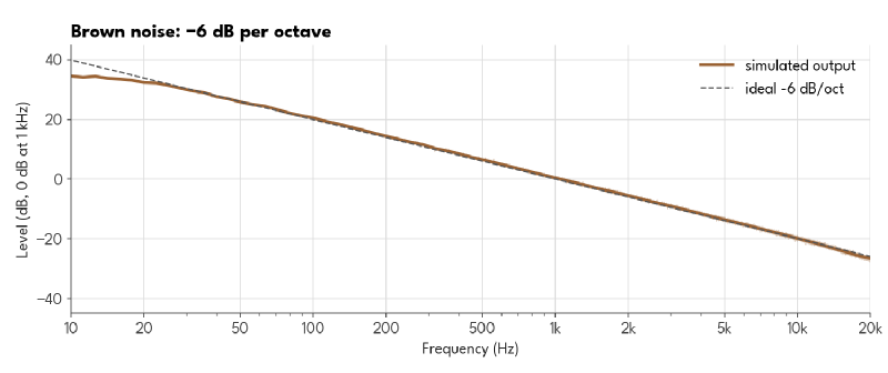
6dBper octave. It sounds deep and rumbling, like surf or distant thunder. Slowed down even further with a slew limiter, it makes a smooth random modulation source.
The spectra below are simulated from the component values of the module. The thin line is the raw spectrum, the thick line is smoothed over 1/6 octave, and the dashed line shows the ideal slope. All three are normalized to 0dB at 1kHz.
How it works#
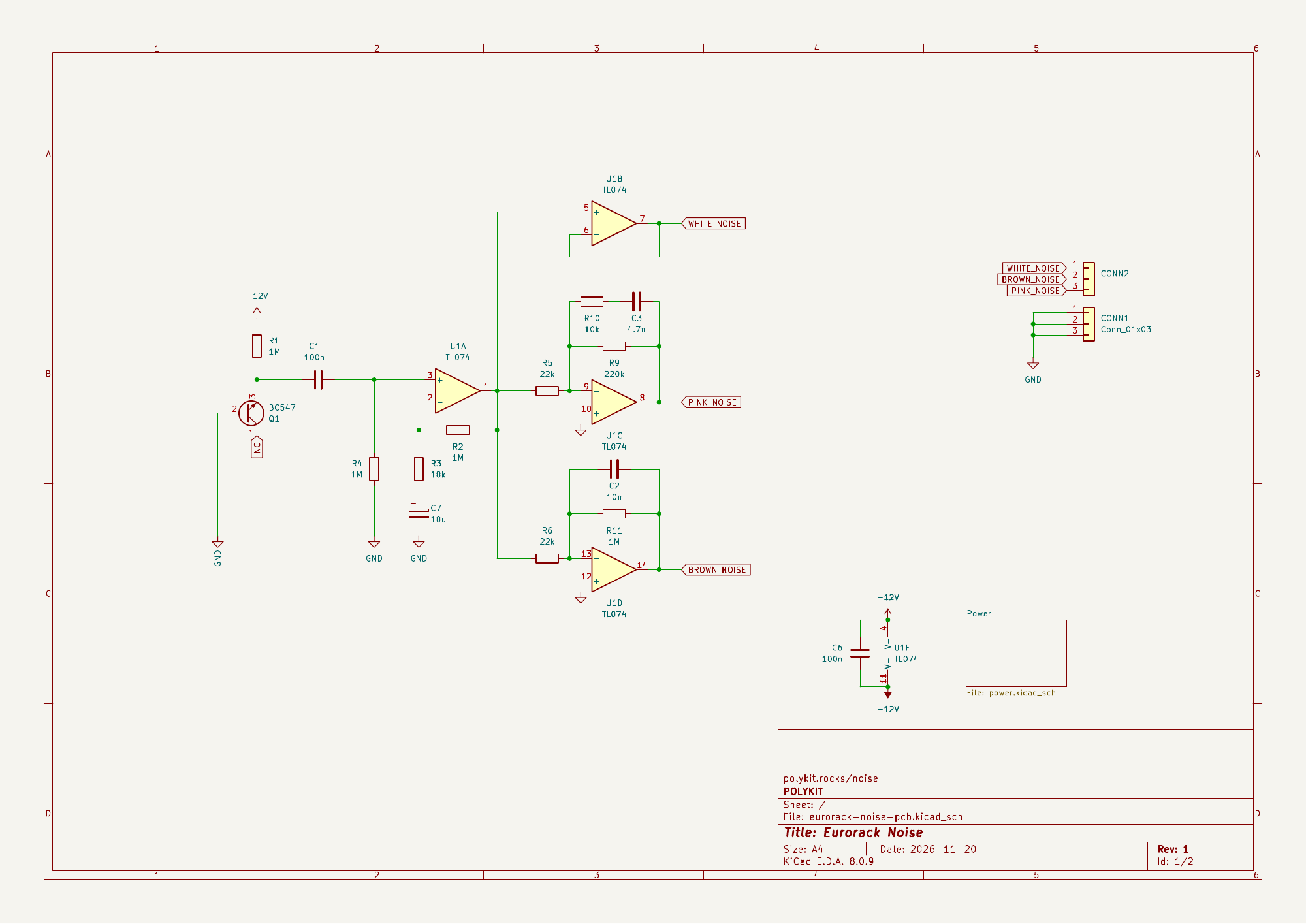
The noise source is a BC547 transistor whose base-emitter junction is reverse-biased through a 1M resistor from +12V. The collector is left unconnected. At around 7 to 9 volts the junction breaks down (avalanche breakdown), and the current through it fluctuates randomly. This produces a small noise signal with a flat spectrum up to well above the audio range.
The first op-amp stage (U1A) amplifies this signal by about 100. A 10µ capacitor in its feedback leg makes the stage work as a plain follower for DC, so the output stays centred around 0V no matter how much DC voltage the transistor produces. A 100n coupling capacitor in front of the stage blocks the transistor’s bias voltage.
The amplified noise feeds three outputs:
- White: U1B buffers the signal unchanged.
- Pink: U1C is an inverting amplifier whose feedback combines a
220kresistor with a10kresistor and4.7ncapacitor in series. Below about150Hzthe gain is 10. Between150Hzand3.4kHzthe capacitor takes over more and more of the feedback and the gain falls. Above that the gain stays at about 0.43. - Brown: U1D is an inverting low-pass filter with a
1Mresistor and a10ncapacitor in the feedback. Above its corner frequency of about16Hzthe output falls at-6dB/octacross the whole audio range.
Filter calculation#
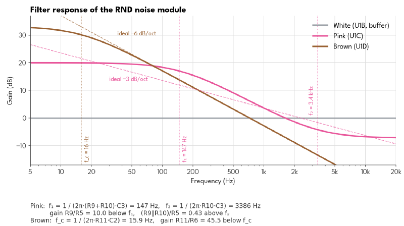
Brown is a first-order low-pass filter. The capacitor C2 shorts the feedback resistor R11 more and more as the frequency rises:
| Formula | Value | |
|---|---|---|
| Gain below the corner | R11 / R6 = 1M / 22k | 45 (+33dB) |
| Corner frequency | fc = 1 / (2π · R11 · C2) = 1 / (2π · 1M · 10n) | 16Hz |
| Slope above the corner | -6dB/oct |
Above 16Hz the gain halves with every octave, which is exactly the brown noise slope. At 1kHz the gain is about 0.7.
Pink needs half that slope, -3dB/oct, and no simple RC filter has it. A single pole falls at -6dB/oct, so the pink filter uses a pole followed by a zero. Between the two, the response tilts down, and with the corners about four octaves apart the average slope comes close to -3dB/oct:
| Formula | Value | |
|---|---|---|
| Gain at low frequencies | R9 / R5 = 220k / 22k | 10 (+20dB) |
| Pole: the slope starts | f1 = 1 / (2π · (R9 + R10) · C3) = 1 / (2π · 230k · 4.7n) | 147Hz |
| Zero: the slope ends | f2 = 1 / (2π · R10 · C3) = 1 / (2π · 10k · 4.7n) | 3.4kHz |
| Gain at high frequencies | (R9 ∥ R10) / R5 = 9.57k / 22k | 0.43 (-7dB) |
Over the audio range the pink output stays within about ±4dB of an ideal pink slope. That is close enough to sound pink, and it needs only one part more than a simple low-pass. A more accurate pink filter would use three or four RC branches with staggered corners.
The gains are chosen so that all three outputs reach roughly the same loudness. The plot shows them relative to the white output, which is the buffered raw noise with a gain of 1.
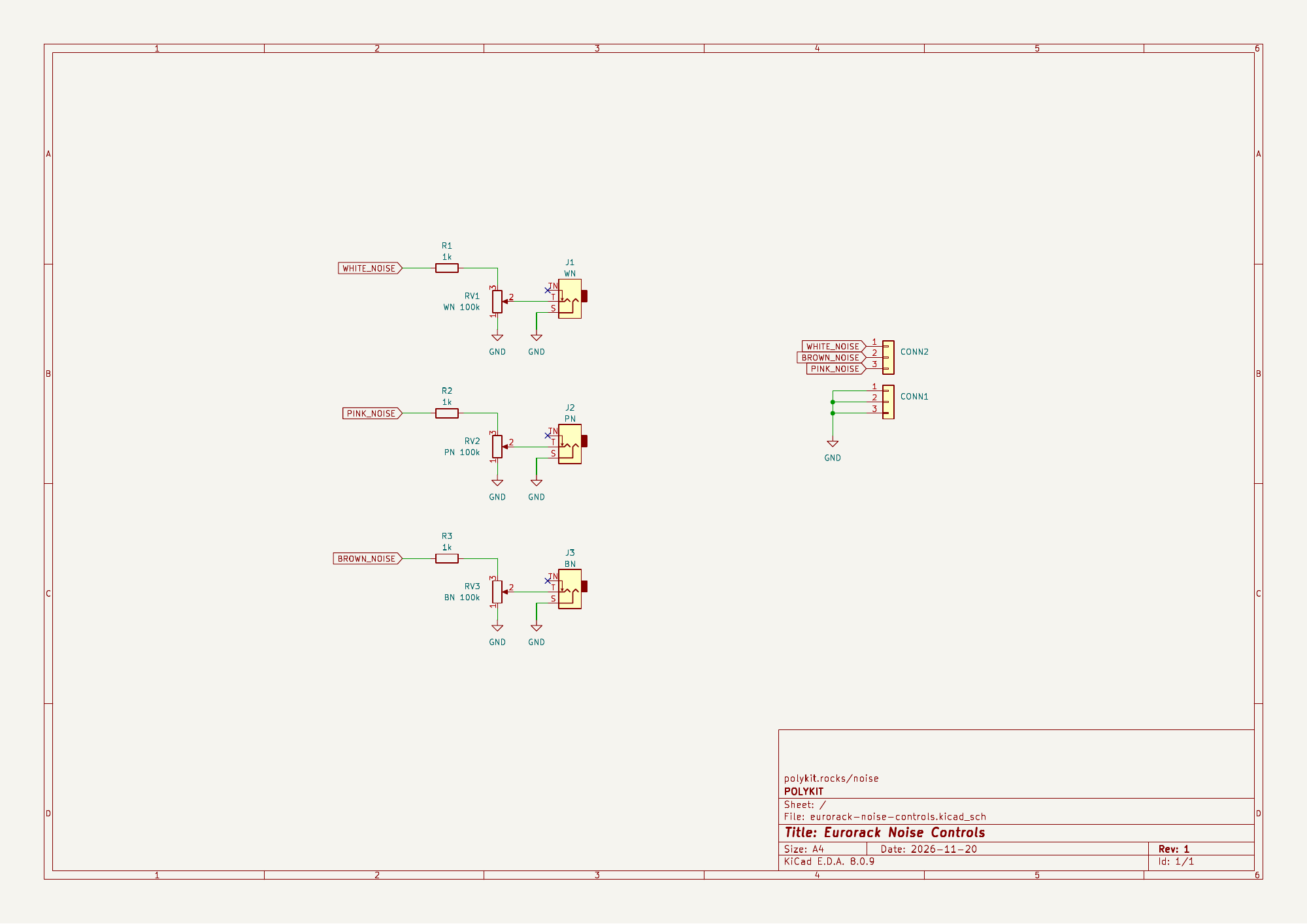
On the control board, every output passes through a 1k resistor to its level potentiometer, whose wiper drives the output jack. As the level control is passive, the outputs work best into the usual high-impedance Eurorack inputs.
The output level depends on the individual transistor, as every BC547 starts to avalanche at a slightly different voltage and produces a slightly different amount of noise.
Experimenting with transistors#
Every transistor type, and even every single transistor, sounds a little different as a noise source: some are louder, some quieter, some give a grainier, crackling noise. If you like to experiment, solder a 2-pin female header into the Q1 position instead of the transistor. Then you can plug in different transistors and compare them. Other small-signal NPN transistors such as the BC548, BC549, 2N3904 or 2N2222 are worth a try.
Mind the pin layout! Only the base and emitter are used; the collector has no pad. The BC547 family has the pinout C-B-E (flat side facing you, legs down), so the collector sits over the missing pad and the base and emitter go into the socket. The 2N3904 and the TO-92 2N2222 have the pinout E-B-C, reversed. Turn them around so that the base and emitter still land in the right holes and the collector leg hangs over the missing pad. Always check the datasheet of your transistor before plugging it in.
Build Guide#
The build is straightforward and well-suited for anyone with basic soldering experience. The module uses only through-hole components, making assembly simple and accessible. The design consists of three PCBs: the front panel, a control/jack board, and the main circuit board.
Start by populating the main circuit board. Begin with the lowest-profile components (resistors, small capacitors) and work your way up to taller parts like the transistor, electrolytic capacitors and the IC socket. The 10-pin power connector goes on the back side of the main board.
The transistor Q1 has only two pins soldered: the pad for the collector is missing on purpose. Bend the collector leg aside or cut it off, and match the flat side of the transistor to the silkscreen.
On the control board, the pin headers go on the back side. Leave the jacks and potentiometers for last.
When mounting the jacks and potentiometers, first place them on the board, then align and secure the front panel before soldering. This ensures proper mechanical alignment and a clean fit. The potentiometers have no threaded bushing; the front panel is held by the jack nuts.
Once all components are soldered, insert the TL074 into its socket — pay close attention to orientation and match the notch on the IC to the marking on the silkscreen.
With the boards fully populated, stack them together using the pin header and socket connections labelled CONN1/CONN1 and CONN2/CONN2. Ensure that all pins are properly aligned before pressing the boards together to avoid bent pins or poor connections.
Each component location is clearly labelled with its designator and value on the PCB silkscreen. Refer to the BOM below for additional details on component types and values.
See the Component Basics guide for help identifying parts.
First Power-On Check#
Before powering the module for the first time, carefully inspect all components, solder joints, and IC orientations.
Check for potential short circuits using a multimeter between -12V, +12V, and ground. For the initial test, it’s best to connect the module to the power supply alone and verify proper operation.
After power-on, give the module a few seconds: the coupling capacitors need a moment to charge before the outputs settle around 0V. Then turn up the knobs and listen to each output through a mixer or an output module. White noise should sound bright, pink noise softer, and brown noise deep and rumbling.
If the noise is very quiet or missing, check the orientation of Q1. A few transistors don’t avalanche well at 12V; swapping Q1 for another BC547 usually helps.
BOM#
Link to interactive BOM of the component board
| Reference | Value | Footprint | Qty | Description |
|---|---|---|---|---|
| C1,C6 | 100n | Capacitor_THT:C_Disc_D5.0mm_W2.5mm_P2.50mm | 2 | Ceramic |
| C2 | 10n | Capacitor_THT:C_Disc_D5.0mm_W2.5mm_P5.00mm | 1 | Ceramic X7R, 5mm pitch |
| C3 | 4.7n | Capacitor_THT:C_Disc_D5.0mm_W2.5mm_P5.00mm | 1 | Ceramic X7R, 5mm pitch |
| C4,C5,C7 | 10u | Capacitor_THT:CP_Radial_D5.0mm_P2.50mm | 3 | Electrolytic |
| CONN1, CONN2 | Conn_01x03 | Connector_PinSocket_2.54mm:PinSocket_1x03_P2.54mm_Vertical | 2 | 3-pin socket, 2.54mm |
| POWER1 | Conn_02x05_Odd_Even | Connector_IDC:IDC-Header_2x05_P2.54mm_Vertical | 1 | IDC 10-pin power connector |
| Q1 | BC547 | Package_TO_SOT_THT:TO-92_Inline_Wide | 1 | NPN transistor, TO-92, collector not connected |
| R1,R2,R4,R11 | 1M | Resistor_THT:R_Axial_DIN0207_L6.3mm_D2.5mm_P2.54mm_Vertical | 4 | 1/4W 1% resistor |
| R3,R10 | 10k | Resistor_THT:R_Axial_DIN0207_L6.3mm_D2.5mm_P2.54mm_Vertical | 2 | 1/4W 1% resistor |
| R5,R6 | 22k | Resistor_THT:R_Axial_DIN0207_L6.3mm_D2.5mm_P2.54mm_Vertical | 2 | 1/4W 1% resistor |
| R7,R8 | 10 | Resistor_THT:R_Axial_DIN0207_L6.3mm_D2.5mm_P2.54mm_Vertical | 2 | 1/4W 1% resistor |
| R9 | 220k | Resistor_THT:R_Axial_DIN0207_L6.3mm_D2.5mm_P2.54mm_Vertical | 1 | 1/4W 1% resistor |
| U1 | TL074 | Package_DIP:DIP-14_W7.62mm | 1 | Quad op-amp, DIP-14, in socket |
Link to interactive BOM of the control board
| Reference | Value | Footprint | Qty | Description |
|---|---|---|---|---|
| CONN1, CONN2 | Conn_01x03 | Connector_PinHeader_2.54mm:PinHeader_1x03_P2.54mm_Vertical | 2 | 3-pin header, 2.54mm |
| J1 | WHITE | Connector_Audio:Jack_3.5mm_QingPu_WQP-PJ398SM_Vertical_CircularHoles | 1 | Mono Thonkiconn 3.5mm jack sockets |
| J2 | PINK | Connector_Audio:Jack_3.5mm_QingPu_WQP-PJ398SM_Vertical_CircularHoles | 1 | Mono Thonkiconn 3.5mm jack sockets |
| J3 | BROWN | Connector_Audio:Jack_3.5mm_QingPu_WQP-PJ398SM_Vertical_CircularHoles | 1 | Mono Thonkiconn 3.5mm jack sockets |
| R1,R2,R3 | 1k | Resistor_THT:R_Axial_DIN0207_L6.3mm_D2.5mm_P2.54mm_Vertical | 3 | 1/4W 1% resistor |
| RV1, RV2, RV3 | 100k | Potentiometer_THT:Potentiometer_Alps_RK09K_Single_Vertical | 3 | Linear, mono, vertical, 6mm shaft, no bushing |
Schematics#
References#
https://www.onsemi.com/download/data-sheet/pdf/bc546-d.pdf
https://www.ti.com/lit/ds/symlink/tl074.pdf